

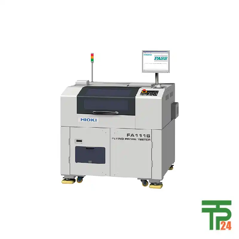
FLYING PROBE TESTER FA1116 HIOKI
- Capacitance Testing Optimized
- Vacuum-Clamp Method
- Reduced-Impact Probes
- Gerber Data Software
Did you like this product? Add to favorites now and follow the product.

(+86) 132-6243-8118 Start Live Chat
Description
Ensuring Flawless Printed Circuit Board Performance
In the relentless march of technological innovation, printed circuit boards (PCBs) stand as the foundational elements powering nearly every electronic device imaginable. From the smallest wearable gadgets to complex industrial machinery and aerospace systems, the integrity and functionality of these boards are paramount. Even a microscopic defect—a hairline short, an open circuit, or a misplaced component—can render an entire system useless, leading to costly recalls, production delays, and reputational damage. Traditional manual inspection methods are insufficient for the intricate, multi-layered PCBs of today. This necessitates automated, high-precision testing solutions capable of verifying electrical continuity and isolation across millions of test points. Flying probe testers have emerged as a critical technology in this domain, offering a flexible, non-contact approach to PCB testing that is essential for ensuring product quality and accelerating time-to-market.
Hioki ATE: The Power to Connect
The Hioki ATE Lineup, specifically highlighted by the FA1116 Flying Probe Tester, embodies “The Power to Connect”—a profound commitment to linking innovation with future reliability. At Hioki, this philosophy translates into a daily dedication to enhancing contact performance, which is the very lifeblood of electrical testing. For PCBs, this means ensuring perfect electrical connection with the circuit board, no matter its complexity or unique characteristics. Hioki’s relentless pursuit is to uncover the true potential of this capability, pushing the boundaries of what testing systems can achieve to support a rich and satisfying lifestyle together with their customers. This is the steadfast path that Hioki follows, recognizing that robust testing systems are not just about defect detection, but about enabling the future of electronics.
The FA1116 represents the pinnacle of this dedication in PCB testing. In a world where electronic products cannot be shipped unless they are verified as non-defective through rigorous testing, the ability to test a wide variety of boards efficiently and accurately becomes the top priority for any tester. The FA1116 achieves this by focusing on its core strengths: adaptability and precision. It’s designed to provide reliable testing solutions that directly contribute to product quality and market readiness. This commitment to continuous improvement in contact performance and overall testing capability ensures that Hioki’s ATE systems are always at the forefront, ready to meet the evolving demands of advanced electronics manufacturing.
Capacitance Testing: Advantages for Speed and Versatility
The Hioki FA1116 Flying Probe Tester leverages the inherent advantages of capacitance testing as an essential technique for optimizing PCB inspection. Capacitance testing is a remarkably effective method for reducing flying probe test times, making it a highly efficient choice for production environments. This technique works by measuring the capacitance between a test point and a reference plane (often ground), or between two test points. Any deviation from the expected capacitance value can indicate an open circuit, a short circuit, or a manufacturing defect. The speed gain comes from the fact that a single capacitance measurement can often verify the integrity of an entire net, rather than requiring individual point-to-point resistance checks, which would be significantly slower.
A paramount advantage of the FA1116’s approach is its vacuum-clamp method. This innovative clamping mechanism allows testing to be carried out without regard to the board shape or the number of layers. This is a critical capability in modern PCB manufacturing, where designs vary widely from rigid multi-layer boards to flexible circuits, and even complex packages like CSPs (Chip Scale Packages). The vacuum-clamp ensures a consistent and stable connection to the board, regardless of its physical characteristics, simplifying setup and increasing reliability. The design philosophy acknowledges that products cannot be shipped unless they are verified as non-defective through testing, and thus, the ability to test various boards is the top priority for a tester. The FA1116 embraces this by allowing testing to be started without concern for factors such as the board’s shape and thickness (be it single-sided, flexible, package, or CSP). While test times are determined by the number of test points and the speed setting (which reflects the extent of impact marks), the FA1116 optimizes these by providing a stable testing environment. This ensures that the instrument’s flexibility in handling diverse board types directly translates into efficient and reliable defect detection across a broad product portfolio, fundamentally contributing to enhanced production throughput and quality assurance.
Single-Sided Testing: Discontinuity and Defect Detection
The Hioki FA1116 Flying Probe Tester further distinguishes itself through the specific advantages of single-sided vacuum-clamp capacitance testing, particularly for discontinuity testing. While double-sided flying probe testers have their merits, single-sided testing, as implemented by the FA1116, offers unique benefits for specific defect detection scenarios. The primary characteristic of single-sided testing in this context is its ability to conduct continuity testing with other nets. This means that instead of solely checking for shorts or opens within a single net, the system can efficiently verify the electrical connection between different nets on the PCB. This is particularly valuable for detecting subtle disconnections or undesired connections between various parts of the circuit.
A common challenge with double-sided contact flying probe testers is that it may not be possible to test some points effectively by means of capacitance measurement alone, depending on the ground plane that is set as the reference. For instance, if a short occurs between two layers that share the same reference plane on a double-sided tester, it might be difficult to isolate. The FA1116 overcomes this by leveraging its single-sided vacuum-clamp method. For example, shorts between boards can be reliably detected as long as the same reference electrode is clamped. This capability ensures that even complex short circuits that might span across different layers or involve the board’s internal structure can be precisely identified. This focused approach to single-sided capacitance testing allows the FA1116 to provide a powerful and reliable method for discontinuity testing, which is crucial for verifying the integrity of complex, multi-layered PCBs. By effectively detecting both open circuits and short circuits that might be challenging for other methods, the FA1116 significantly enhances the comprehensiveness of PCB electrical testing, contributing to superior product quality and reduced manufacturing defects.
Optimizing Speed: Stable Impact and Reduced Marks
The Hioki FA1116 Flying Probe Tester achieves its high-speed testing capabilities while also addressing a critical practical concern in PCB manufacturing: stable impact marks and high-speed testing. Inevitably, electrical testing involves probe impact marks on the circuit board. While unavoidable, minimizing their impact and ensuring consistency is key. For a tester, it’s easier to set fixed conditions if the measurement target itself conforms to fixed parameters. However, modern PCBs are diverse. The FA1116’s design focuses on simplifying the probe contact mechanism, which is often complex in double-sided contact testing where ascertaining the state of the contact surface can be difficult.
By having a uniform test surface with its single-sided vacuum-clamp method, the FA1116 allows for rapid specification of various conditions conceived to minimize test times (for example, speed and the amount of downward probe force). This streamlined approach means the design eliminates the need to use a contact check function or test surface height correction, which are often time-consuming steps in other testers. This simplification of testing procedures directly contributes to shortening the ultimate test time. Furthermore, for delicate fine pattern testing, the FA1116 offers reduced-impact link probes (optional). By combining these newly designed reduced-impact probes with precision soft-landing control, the FA1116-03 model makes it possible to approach the maximum speed setting during fine pattern testing without causing excessive damage or noticeable marks on sensitive circuit features. This balance of speed, minimal impact, and simplified operation ensures that the FA1116 delivers efficient and reliable testing even for the most advanced and delicate PCB designs, safeguarding product aesthetics and integrity while maintaining high throughput.
Comprehensive Software and Probe Lineup
The efficacy of a flying probe tester extends beyond its hardware capabilities; robust software and a versatile probe selection are equally critical. The Hioki FA1116 Flying Probe Tester is supported by a comprehensive software and probe lineup, ensuring adaptability to a wide range of PCB testing scenarios and streamlined data management. The probe lineup itself is extensive: users can select from an extensive range of variations based on the types of boards they wish to test. This flexibility ensures that regardless of the PCB’s material, pad size, or test point density, there’s an optimal probe available to achieve precise and reliable contact without damaging the board. This customization is essential for addressing the diverse and evolving landscape of PCB designs.
On the software front, Hioki provides powerful tools for both test data creation and defect analysis. To streamline test program generation, Hioki developed its own proprietary software for editing Gerber data with the FEB-LINE UA1781. This software, a successor to the acclaimed Fly-Line, incorporates the testing expertise necessary to create flying-probe data with proprietary functionality that facilitates tasks that would be troublesome with conventional editing software. This includes specialized features for handling cavity data (relevant for recessed features on PCBs) and processing of net connections for paint data (used for selective coating or mask application). This tailored software simplifies the often complex process of preparing test data, reducing setup time and potential errors. For post-test analysis, the FAIL VISUALIZER UA1782 is indispensable. This viewer software displays defective nets and searches for defect locations based on the results of capacitance measurement. By visually highlighting problem areas on a graphical representation of the PCB, it drastically speeds up defect diagnosis and facilitates efficient repair, transforming raw measurement data into actionable insights for quality improvement. This integrated hardware and software ecosystem ensures that the FA1116 provides a complete, efficient, and user-friendly solution for advanced PCB testing.
Unwavering Quality: Japanese Engineering Excellence
The Hioki FA1116 Flying Probe Tester embodies a fundamental commitment to unwavering quality, a hallmark of Hioki’s renowned Japanese engineering excellence. The company’s philosophy, “The Power to Connect,” extends deeply into its manufacturing processes, focusing on creating reliable, precise, and durable test systems. While the specific manufacturing location for the FA1116 is not detailed in the provided text, Hioki’s strong reputation for designing and manufacturing its products in Japan, as seen with other instruments, suggests that the FA1116 benefits from similar rigorous standards. This implies that the entire development, design, and manufacturing processes for this sophisticated PCB testing system are meticulously carried out with exceptional attention to detail, likely at Hioki’s advanced facilities in Nagano Prefecture, Japan.
This vertically integrated approach allows Hioki to maintain absolute control over every stage of production, from the selection of high-grade components to the intricate assembly of precision mechanics and optics, to the precise calibration of electrical measurement circuits. By leveraging some of the industry’s most advanced technological capabilities, Hioki consistently delivers products of the highest possible quality. For a flying probe tester, this translates into exceptional measurement accuracy and repeatability, long-term operational stability, and robust durability even under continuous, high-volume industrial use. The precision of the probe movements, the consistency of the vacuum-clamp system, and the reliability of the electrical measurements are all outcomes of this commitment to engineering excellence. This dedication to quality is not merely a feature; it provides profound peace of mind for manufacturers who rely on these instruments for critical quality control. Knowing that a key testing system is built to the highest possible standards minimizes concerns about equipment malfunction, false readings, or premature failure, which could lead to costly production downtime or product recalls. The FA1116’s robust build ensures that it is a dependable workhorse, contributing significantly to a secure and efficient PCB manufacturing environment.
tpt24.com: Your Premier Global Source
In the demanding world of printed circuit board manufacturing and electronics assembly, where precision, speed, and reliability are paramount, acquiring a state-of-the-art instrument like the Hioki FA1116 Flying Probe Tester demands a supplier that embodies expertise, trust, and global reach. tpt24.com proudly stands as the world’s leading online store for this exceptional product line. Our unwavering commitment is to provide you with a seamless acquisition experience, fortified by an absolute guarantee of authenticity and an uncompromising dedication to quality for every product we deliver. We deeply understand that the integrity of your PCBs, the efficiency of your production lines, and the reputation of your brand hinge fundamentally on the accuracy and longevity of the test equipment you employ. Therefore, every Hioki FA1116 unit, along with its specialized probes (including reduced-impact link probes) and essential software (FEB-LINE UA1781, FAIL VISUALIZER UA1782), sourced through tpt24.com, is meticulously guaranteed to be a genuine Hioki product. These instruments are manufactured to the most stringent industry standards and rigorously tested to ensure peak performance, consistently delivering the precise and rapid PCB testing you demand for your critical applications.
What truly sets tpt24.com apart is our profound commitment to global accessibility. We firmly believe that geographical location should never be a barrier to acquiring the world’s most advanced test and measurement technology. Consequently, tpt24.com offers swift and secure worldwide delivery of the Hioki FA1116 Flying Probe Tester to any country you operate in. Our robust and highly efficient global logistics network ensures that your valuable investment is handled with the utmost care, processed promptly, and dispatched efficiently, arriving at your facility in pristine condition and within a predictable timeframe. We fully appreciate the time-sensitive nature of modern electronics manufacturing, where high throughput and uncompromising quality control are essential, and the urgency often associated with implementing critical PCB testing solutions. Our streamlined online purchasing experience, coupled with our dependable international shipping capabilities, is meticulously designed to minimize any potential delays, enabling you to integrate this powerful instrument into your production line or R&D laboratory with maximum speed and efficiency. When you choose tpt24.com, you are selecting a trusted global partner, committed to providing you with not only cutting-edge technology but also unparalleled service, absolute product authenticity, guaranteed quality, and reliable worldwide delivery. Your journey towards unparalleled PCB quality and manufacturing efficiency begins here, with the confidence that comes from sourcing your equipment from the world’s best.
Specifications
| Number of arms | 2 | |||||
|---|---|---|---|---|---|---|
| Number of test steps | Max. 40,000 steps/piece 300,000 steps/sheet |
|||||
| DC Measurement ranges | Resistance : 400 μΩ to 40 MΩ Capacitance : 4 μF to 40 mF Diode, transistor (VF) : 0 to 25 V Zener diode (VZ) : 0 to 25 V Short :400 mΩ to 40 kΩ Open :4 Ω to 4 MΩ Voltage :0 to 25 V |
|||||
| AC Measurement ranges | Resistance : 100 Ω to 100 MΩ Capacitance : 10 fF to 10 μF Inductance : 10 μH to 100 mH |
|||||
| Measurement time | Max. 100 points/s (X-Y movements of 0.1 mm, 2 arm simultaneous probing, capacitance measurement) | |||||
| Probe working area | 610 mm (24.02 in) W × 510 mm (20.08 in) D | |||||
| Fixed board dimensions | Thickness : 0.1 mm to 3.2 mm (0.13 in) Outer dimensions : 50 mm (1.97 in) W × 50 mm (1.97 in) D to 610 mm (24.02 in) W × 510 mm (20.08 in) D Upper surface – 10 mm (0.39 in) (including board thickness) Lower surface – 0.1 mm (0.00 in) |
|||||
| Board-carrier | N/A | |||||
| Power supply | 200 V AC ±10% (single-phase), 50/60 Hz, 3 kVA | |||||
| Dimensions and mass | 1,443 mm (56.81 in) W × 1,656 mm (65.20 in) H × 1,185 mm (46.65 in) D, 1,000 kg (35,273.4 oz) | |||||
Related products


Recently Viewed Products

krohne OPTIWAVE 5400
UNI-T UT372 Tachometers
FLIR T540 Handheld Thermal Camera

krohne OPTISONIC 4400 HP

Fair Pricing, Guarantee of Authenticity and Quality, Fast Delivery, and Provision of Technical Support to Customers.
Copyright 2025 © TPT24 Company. All right reserved. Powered by TPT24.
